Digital VLSI Design and Simulation with Verilog Suman 1st edition by Lata Tripathi, Sobhit Saxena, Sanjeet Sinha, Govind Patel 1119778080 9781119778080
$50.00 Original price was: $50.00.$25.00Current price is: $25.00.
Digital VLSI Design and Simulation with Verilog Suman 1st edition by Lata Tripathi, Sobhit Saxena, Sanjeet K. Sinha, Govind S Patel – Ebook PDF Instant Download/DeliveryISBN: 1119778080, 9781119778080
Full download Digital VLSI Design and Simulation with Verilog Suman 1st edition after payment.
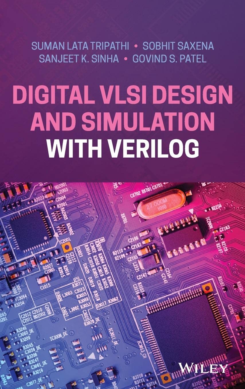
Product details:
ISBN-10 : 1119778080
ISBN-13 : 9781119778080
Author : Lata Tripathi, Sobhit Saxena, Sanjeet K. Sinha, Govind S Patel
Digital VLSI Design Problems and Solution with Verilog delivers an expertly crafted treatment of the fundamental concepts of digital design and digital design verification with Verilog HDL. The book includes the foundational knowledge that is crucial for beginners to grasp, along with more advanced coverage suitable for research students working in the area of VLSI design. Including digital design information from the switch level to FPGA-based implementation using hardware description language (HDL), the distinguished authors have created a one-stop resource for anyone in the field of VLSI design.
Digital VLSI Design and Simulation with Verilog Suman 1st Table of contents:
1 Combinational Circuit Design
1.1 Logic Gates
1.1.1 Universal Gate Operation
1.1.2 Combinational Logic Circuits
1.2 Combinational Logic Circuits Using MSI
1.2.1 Adders
1.2.2 Multiplexers
1.2.3 De-multiplexer
1.2.4 Decoders
1.2.5 Multiplier
1.2.6 Comparators
1.2.7 Code Converters
1.2.8 Decimal to BCD Encoder
Review Questions
Multiple Choice Questions
Reference
2 Sequential Circuit Design
2.1 Flip-flops (F/F)
2.1.1 S-R F/F
2.1.2 D F/F
2.1.3 J-K F/F
2.1.4 T F/F
2.1.5 F/F Excitation Table
2.1.6 F/F Characteristic Table
2.2 Registers
2.2.1 Serial I/P and Serial O/P (SISO)
2.2.2 Serial Input and Parallel Output (SIPO)
2.2.3 Parallel Input and Parallel Output (PIPO)
2.2.4 Parallel Input and Serial Output (PISO)
2.3 Counters
2.3.1 Synchronous Counter
2.3.2 Asynchronous Counter
2.3.3 Design of a 3-Bit Synchronous Up-counter
2.3.4 Ring Counter
2.3.5 Johnson Counter
2.4 Finite State Machine (FSM)
2.4.1 Mealy and Moore Machine
2.4.2 Pattern or Sequence Detector
Review Questions
Multiple Choice Questions
Reference
3 Introduction to Verilog HDL
3.1 Basics of Verilog HDL
3.1.1 Introduction to VLSI
3.1.2 Analog and Digital VLSI
3.1.3 Machine Language and HDLs
3.1.4 Design Methodologies
3.1.5 Design Flow
3.2 Level of Abstractions and Modeling Concepts
3.2.1 Gate Level
3.2.2 Dataflow Level
3.2.3 Behavioral Level
3.2.4 Switch Level
3.3 Basics (Lexical) Conventions
3.3.1 Comments
3.3.2 Whitespace
3.3.3 Identifiers
3.3.4 Escaped Identifiers
3.3.5 Keywords
3.3.6 Strings
3.3.7 Operators
3.3.8 Numbers
3.4 Data Types
3.4.1 Values
3.4.2 Nets
3.4.3 Registers
3.4.4 Vectors
3.4.5 Integer Data Type
3.4.6 Real Data Type
3.4.7 Time Data Type
3.4.8 Arrays
3.4.9 Memories
3.5 Testbench Concept
Multiple Choice Questions
References
4 Programming Techniques in Verilog I
4.1 Programming Techniques in Verilog I
4.2 Gate-Level Model of Circuits
4.3 Combinational Circuits
4.3.1 Adder and Subtractor
4.3.2 Multiplexer and De-multiplexer
4.3.3 Decoder and Encoder
4.3.4 Comparator
Review Questions
Multiple Choice Questions
References
5 Programming Techniques in Verilog II
5.1 Programming Techniques in Verilog II
5.2 Dataflow Model of Circuits
5.3 Dataflow Model of Combinational Circuits
5.3.1 Adder and Subtractor
5.3.2 Multiplexer
5.3.3 Decoder
5.3.4 Comparator
5.4 Testbench
5.4.1 Dataflow Model of the Half Adder and Testbench
5.4.2 Dataflow Model of the Half Subtractor and Testbench
5.4.3 Dataflow Model of 2 × 1 Mux and Testbench
5.4.4 Dataflow Model of 4 × 1 Mux and Testbench
5.4.5 Dataflow Model of 2-to-4 Decoder and Testbench
Review Questions
Multiple Choice Questions
References
6 Programming Techniques in Verilog II
6.1 Programming Techniques in Verilog II
6.2 Behavioral Model of Combinational Circuits
6.2.1 Behavioral Code of a Half Adder Using If-else
6.2.2 Behavioral Code of a Full Adder Using Half Adders
6.2.3 Behavioral Code of a 4-bit Full Adder (FA)
6.2.4 Behavioral Model of Multiplexer Circuits
6.2.5 Behavioral Model of a 2-to-4 Decoder
6.2.6 Behavioral Model of a 4-to-2 Encoder
6.3 Behavioral Model of Sequential Circuits
6.3.1 Behavioral Modeling of the D-Latch
6.3.2 Behavioral Modeling of the D-F/F
6.3.3 Behavioral Modeling of the J-K F/F
6.3.4 Behavioral Modeling of the D-F/F Using J-K F/F
6.3.5 Behavioral Modeling of the T-F/F Using J-K F/F
6.3.6 Behavior Modeling of an S-R F/F Using J-K F/F
Review Questions
Multiple Choice Questions
References
7 Digital Design Using Switches
7.1 Switch-Level Model
7.2 Digital Design Using CMOS Technology
7.3 CMOS Inverter
7.4 Design and Implementation of the Combinational Circuit Using Switches
7.4.1 Types of Switches
7.4.2 CMOS Switches
7.4.3 Resistive Switches
7.4.4 Bidirectional Switches
7.4.5 Supply and Ground Requirements
7.5 Logic Implementation Using Switches
7.5.1 Digital Design with a Transmission Gate
7.6 Implementation with Bidirectional Switches
7.6.1 Multiplexer Using Switches
7.7 Verilog Switch-Level Description with Structural-Level Modeling
7.8 Delay Model with Switches
Review Questions
Multiple Choice Questions
References
8 Advance Verilog Topics
8.1 Delay Modeling and Programming
8.1.1 Delay Modeling
8.1.2 Distributed-Delay Model
8.1.3 Lumped-Delay Model
8.1.4 Pin-to-Pin-Delay Model
8.2 User-Defined Primitive (UDP)
8.2.1 Combinational UDPs
8.2.2 Sequential UDPs
8.2.3 Shorthands in UDP
8.3 Task and Function
8.3.1 Difference between Task and Function
8.3.2 Syntax of Task and Function Declaration
8.3.3 Invoking Task and Function
8.3.4 Examples of Task Declaration and Invocation
8.3.5 Examples of Function Declaration and Invocation
Review Questions
Multiple Choice Questions
References
9 Programmable and Reconfigurable Devices
9.1 Logic Synthesis
9.1.1 Technology Mapping
9.1.2 Technology Libraries
9.2 Introduction of a Programmable Logic Device
9.2.1 PROM, PAL and PLA
9.2.2 SPLD and CPLD
9.3 Field-Programmable Gate Array
9.3.1 FPGA Architecture
9.4 Shannon’s Expansion and Look-up Table
9.4.1 2-Input LUT
9.4.2 3-Input LUT
9.5 FPGA Families
9.6 Programming with FPGA
9.6.1 Introduction to Xilinx Vivado Design Suite for FPGA-Based Implementations
9.7 ASIC and Its Applications
Review Questions
Multiple Choice Questions
References
10 Project Based on Verilog HDLs
10.1 Project Based on Combinational Circuit Design Using Verilog HDL
10.1.1 Full Adder Using Switches at Structural Level Model
10.1.2 Ripple-Carry Full Adder (RCFA)
10.1.3 4-bit Carry Look-ahead Adder (CLA)
10.1.4 Design of a 4-bit Carry Save Adder (CSA)
10.1.5 2-bit Array Multiplier
10.1.6 2 × 2 Bit Division Circuit Design
10.1.7 2-bit Comparator
10.1.8 16-bit Arithmetic Logic Unit
10.1.9 Design and Implementation of 4 × 16 Decoder Using 2 × Decoder
10.2 Project Based on Sequential Circuit Design Using Verilog HDL
10.2.1 Design of 4-bit Up/down Counter
10.2.2 LFSR Based 8-bit Test Pattern Generator
10.3 Counter Design
10.3.1 Random Counter that Counts Sequence like 2,4,6,8,2,8…and so On
10.3.2 Use of Task at the Behavioral-Level Model
10.3.3 Traffic Signal Light Controller
10.3.4 Hamming Code(h,k) Encoder/Decoder
Review Questions
Multiple Choice Questions
References
11 SystemVerilog
11.1 Introduction
11.2 Distinct Features of SystemVerilog
11.2.1 Data Types
11.2.2 Arrays
11.2.3 Typedef
11.2.4 Enum
11.3 Always_type
11.4 $log2c() Function
11.5 System-Verilog as a Verification Language
People also search for Digital VLSI Design and Simulation with Verilog Suman 1st:
digital circuit design using verilog
digital design using digilent fpga boards verilog pdf
digital systems design using verilog solution manual pdf
digital vlsi design and simulation with verilog
digital vlsi design with verilog a textbook from silicon valley
Tags: Design, Digital, Simulation, Verilog Suman, Lata Tripathi, Sobhit Saxena, Sanjeet Sinha, Govind Patel
You may also like…
Engineering - Electrical & Electronic Engineering
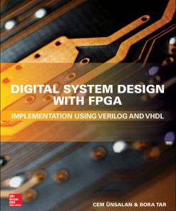
Digital System Design with FPGA: Implementation Using Verilog and VHDL 1st Edition
Engineering - Energy & Power Resources
Green Energy: Solar Energy, Photovoltaics, and Smart Cities 1st Edition Suman Lata Tripathi
Engineering - Electrical & Electronic Engineering
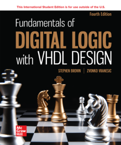
Fundamentals of Digital Logic with VHDL Design 4th Edition by Brown 1260597784 978-1260597783
Mathematics - Wavelets and signal processing
Engineering - Aerospace Engineering
Flight Simulation Software: Design, Development and Testing 1st Edition David Allerton
Computers - Computer Graphics & Design


![Design Recipes for FPGAs using Verilog and VHDL [2nd ed.] Peter Wilson](https://ebookmass.com/wp-content/uploads/2024/04/design-recipes-for-fpgas-using-verilog-and-vhdl-2nd-ed-7259972-247x296.jpg)
